
Facilities
Our laboratory is dedicated to advancing the understanding of light–matter interactions in optoelectronic materials, with a strong emphasis on both fundamental studies and device-level optimization. We integrate device fabrication with a comprehensive suite of optical and electrical characterization techniques to explore and enhance the performance of next-generation optoelectronic devices.
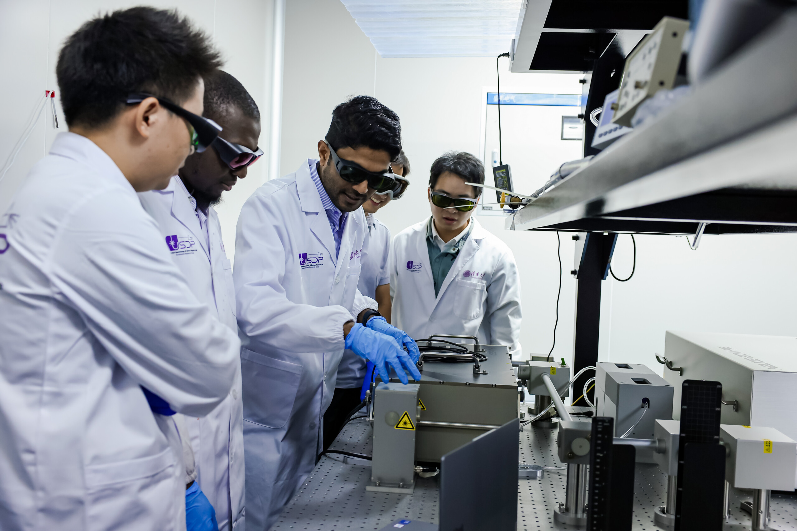
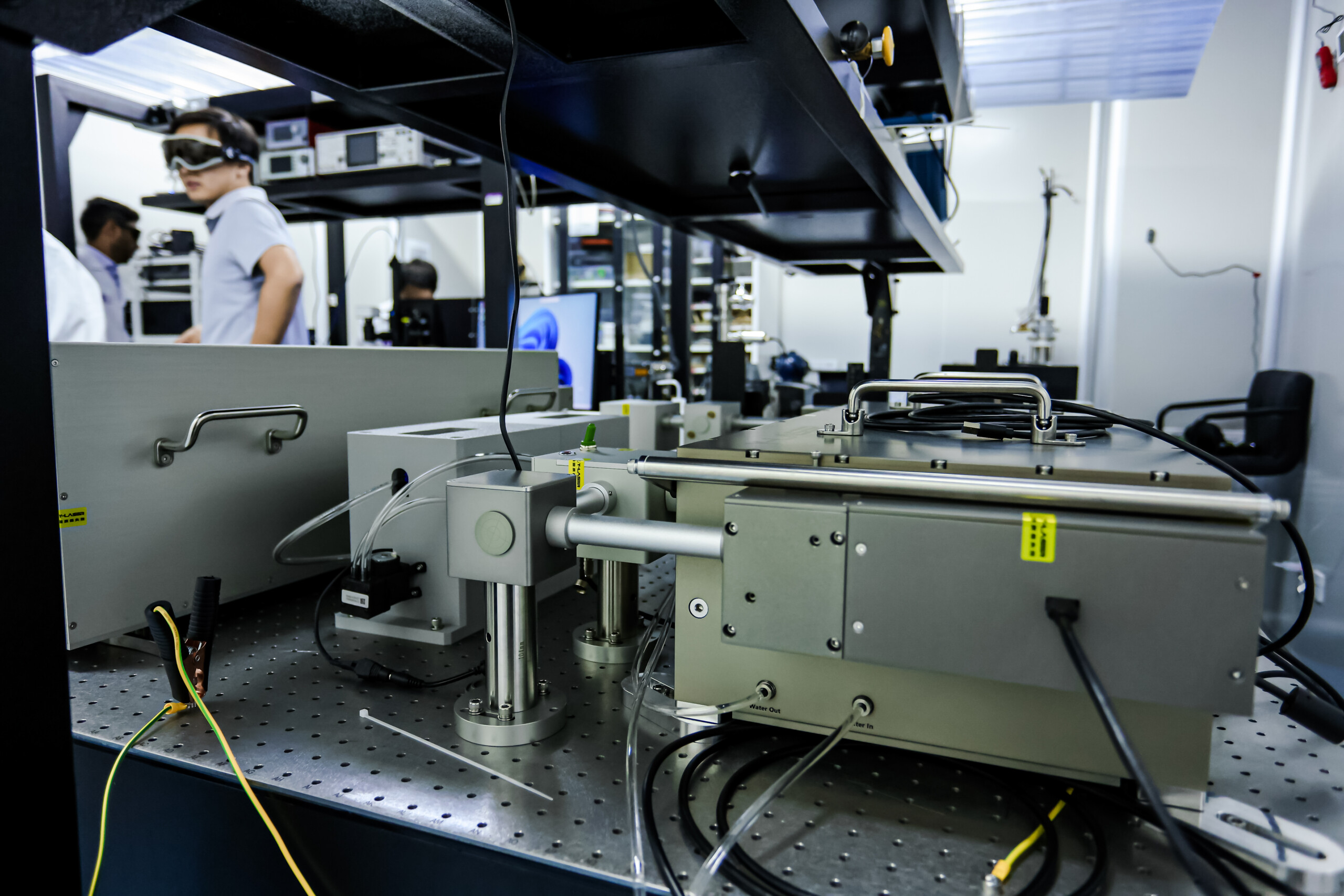
We specialize in ultrafast spectroscopic techniques, particularly transient absorption (TA) and transient reflection (TR) spectroscopy, which enable us to track excited-state dynamics across a broad temporal range—from femtoseconds to microseconds (fs–ns–μs). These measurements provide critical insights into exciton generation, charge transfer, and recombination dynamics, which are central to the operation of high-performance photovoltaic and light-emitting devices.
To probe charge dynamics at the device level, we employ Transient Photovoltage (TPV) and Transient Photocurrent (TPC) techniques, revealing charge carrier lifetimes and transport behavior under operating conditions. Impedance Spectroscopy (IS) is used to assess internal resistance, capacitance, and interfacial quality, while JV (current–voltage) characterization offers key performance indicators such as power conversion efficiency, fill factor, and stability.


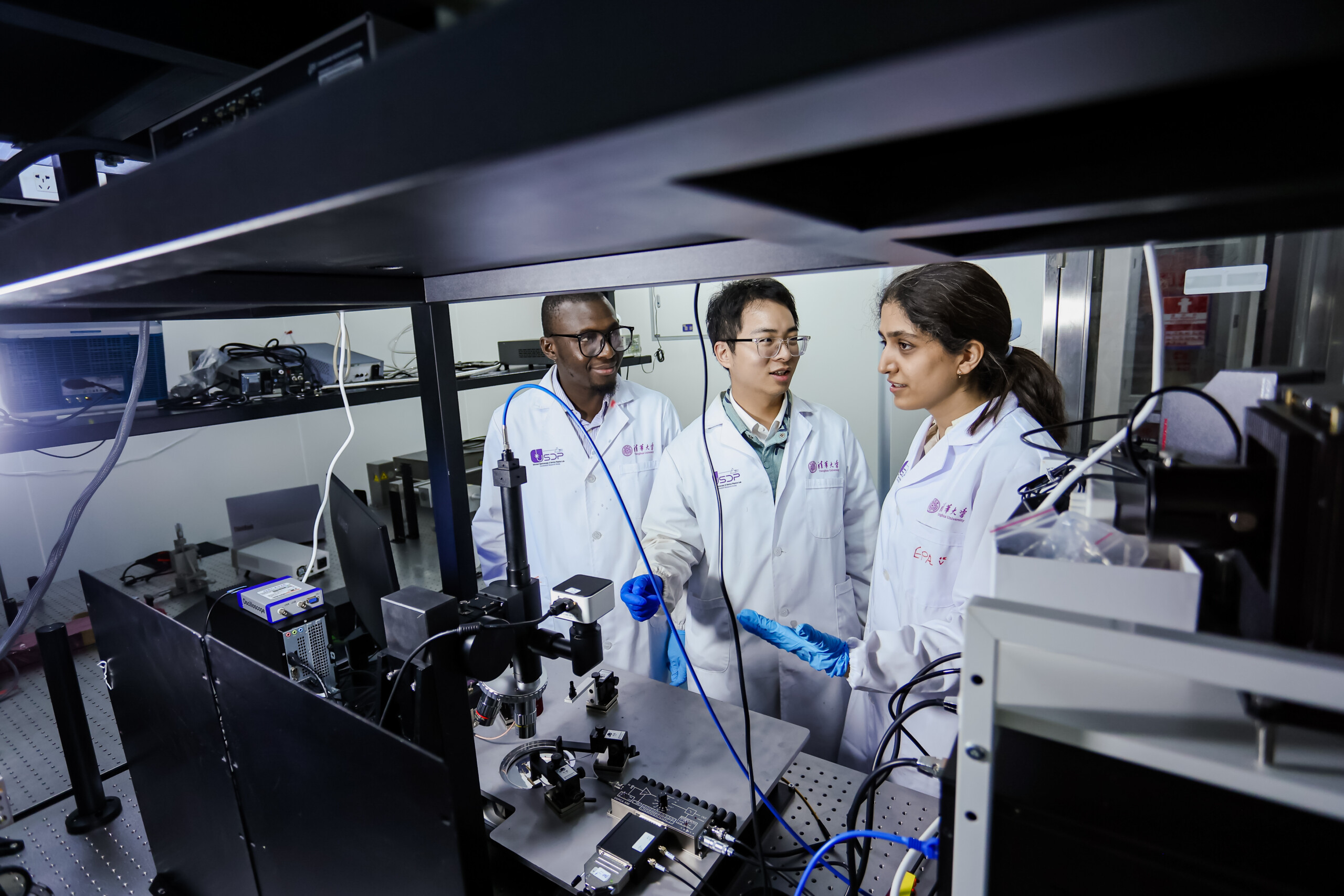
For emission and energy loss studies, Electroluminescence (EL) and Photoluminescence (PL) measurements provide valuable information about radiative recombination pathways, particularly relevant for studying the energy losses in organic photovoltaics.
Complementing these dynamic techniques, we carry out thin film and steady-state optical characterizations. UV–Visible (UV-Vis) spectroscopy and Photoluminescence (PL) measurements elucidate absorption/emission profiles and bandgap energies. Photoluminescence Quantum Yield (PLQY) measurements allow us to quantify radiative efficiencies, while contact angle analysis helps evaluate surface wettability and film uniformity—critical for stable multilayer device structures.
Our fabrication facilities include nitrogen-filled gloveboxes for processing air-sensitive materials under inert conditions, ensuring consistent film quality. Physical Vapor Deposition (PVD) systems allow for precise deposition of electrodes, charge transport layers, and active layers, enabling nanometer-scale control over device architecture.
Together, these capabilities form a comprehensive platform for the fabrication and analysis of advanced optoelectronic devices, bridging material science and device physics. Our infrastructure supports in-depth investigations into material innovations, performance optimization, and long-term stability—driving progress in organic solar cells, perovskite photovoltaics, 2-Dimensional materials, and other emerging optoelectronic technologies.